ULP Footprint
KiCad Footprints for Cherry Ultra Low Profile Switches
Why yet another footprint
Cherry makes very nice ultra low profile switches, for which I have designed a few boards (see projects). There are footprints made for SMD-soldering and handsoldering, however, I was not happy with the handsolder-footprint, as its slit design makes it harder than necessary to see whether a switch is correctly soldered. I took inspirations of Geist's XIAO-footprint with a big cutout in the bottom, to make soldering the pad on the bottom of the component easier and applied the same trick to the Cherry ULP-footprint.
Big thanks to Hendrick for integrating 3d models into the footprints, and to Fooker for the keycap model.
Solderguide
Soldering of the switches has to be done with care. The footprint is designed for handsoldering therefore I recommend against using a hotplate. Start by placing the switch on the PCB and soldering at least one of the accessible solder pads from the top (i.e. the side you type on) such that the switch is mechanically secure. Then flip the PCB around. You should see the bottom of the PCB and the cutout in the PCB for the central pads of the switch. Solder the pads on the PCB as well as the ones through the cutout. Be careful not to use to much solder when soldering the pads of the switches. If you use too much solder the switch will not work anymore. Try with one and see whether it still works before soldering in all the switches and potentially ruining all your switches.
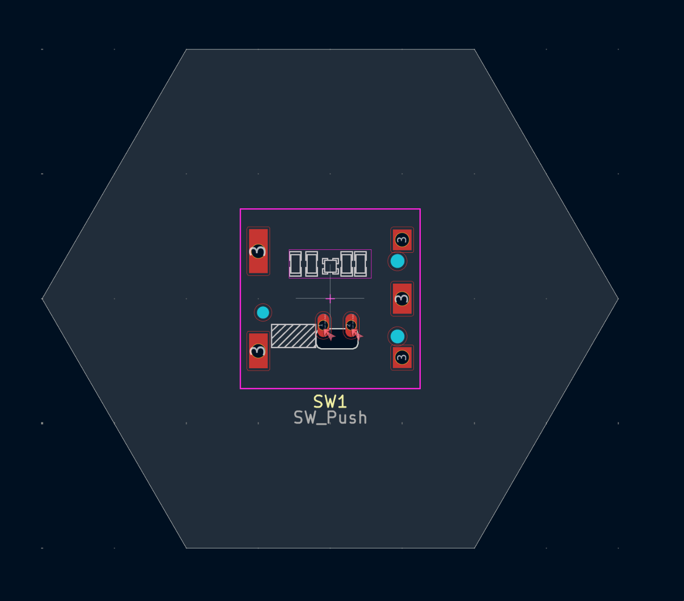
Design Problems
The cutout has to overlap with the solderpads of the switch to function properly. This, however, causes 2 Board edge clearance violation DRC-errors per switch in KiCad (see the two red arrows in the screenshot blow). You can safely ignore these errors.
If you know a good way to circumvent these errors, please contact me.